| Sep 09, 2022 |
|
(Nanowerk Information) A family microwave oven modified by a Cornell Engineering professor helps to prepare dinner up the subsequent technology of cellphones, computer systems and different electronics after the invention was proven to beat a serious problem confronted by the semiconductor trade.
|
|
The analysis is detailed in a paper in Utilized Physics Letters (“Environment friendly and steady activation by microwave annealing of nanosheet silicon doped with phosphorus above its solubility restrict”). The lead writer is James Hwang, a analysis professor within the Division of Supplies Science and Engineering; different Cornell contributors are doctoral pupil Chandrasekhar Savant and former postdoctoral researcher Mohammed Javad Asadi.
|
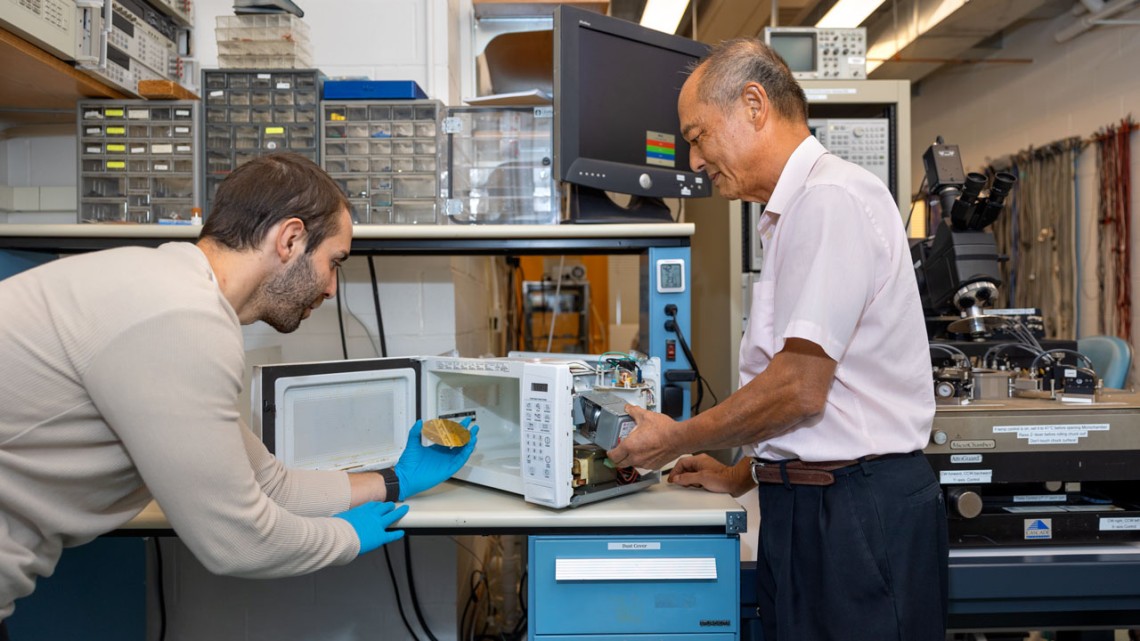 |
| James Hwang, analysis professor within the Division of Supplies Science and Engineering, proper, at his modified microwave with Gianluca Fabi holding a semiconductor at left. (Picture: Ryan Younger, Cornell College)
|
|
Producing the supplies that make up transistors and different microchip parts is much like baking in that materials components have to be combined collectively after which heated, amongst different steps, with the intention to produce a desired electrical present. As an illustration, phosphorus is added to silicon after which the combination is annealed, or heated, to place the phosphorus atoms into the proper place in order that they’re lively in present conduction.
|
|
However as microchips proceed to shrink, the silicon have to be doped, or combined, with larger concentrations of phosphorus to provide the specified present. Semiconductor producers are actually approaching a essential restrict through which heating the extremely doped supplies utilizing conventional strategies now not produces constantly useful semiconductors.
|
|
“We want concentrations of phosphorus which can be larger than its equilibrium solubility in silicon. That goes towards nature,” Hwang stated. “The silicon crystal expands, inflicting immense pressure and making it probably ineffective for electronics.”
|
|
The Taiwan Semiconductor Manufacturing Firm (TSMC) had theorized that microwaves may very well be used to activate the surplus dopants, however similar to with family microwave ovens that generally warmth meals erratically, earlier microwave annealers produced “standing waves” that prevented constant dopant activation. So TSMC partnered with Hwang, who modified a microwave oven to selectively management the place the standing waves happen. Such precision permits for the right activation of the dopants with out extreme heating or injury of the silicon crystal.
|
|
This discovery may very well be used to provide semiconductor supplies and electronics showing across the 12 months 2025, stated Hwang, who has filed two patents for the prototype microwave annealer with postdoctoral researcher Gianluca Fabi.
|
|
“Just a few producers are presently producing semiconductor supplies which can be 3 nanometers,” Hwang stated. “This new microwave method can probably allow main producers reminiscent of TSMC and Samsung to scale down to only 2 nanometers.”
|
|
The breakthrough may change the geometry of transistors utilized in microchips. For greater than 20 years, transistors have been made to face up like dorsal fins in order that extra may be packed on every microchip, however producers have lately begun to experiment with a brand new structure through which transistors are stacked horizontally as nanosheets that may additional enhance the density and management of transistors. The excessively doped supplies enabled by microwave annealing could be key to the brand new structure.
|
",
type: "opt-in",
theme: "edgeless",
palette: {
popup: {
background: "#eee",
text: "#889"
},
button: {
background: "#58f",
text: "#fff"
}
},
content: {
link: "Сookie policy",
allow: "Got it!",
deny: " ",
href: "https://www.nanowerk.com/cookie_policy.php"
},
onInitialise: function(status) {
if(status == cookieconsent.status.allow) myScripts();
},
onStatusChange: function(status) {
if (this.hasConsented()) myScripts();
}
})
});
function myScripts() {
// Paste here your scripts that use cookies requiring consent. See examples below
// Google Analytics, you need to change 'UA-00000000-1' to your ID
(function(i,s,o,g,r,a,m))(window,document,'script','//www.google-analytics.com/analytics.js','ga');
ga('create', 'UA-00000000-1', 'auto');
ga('send', 'pageview');
// Facebook Pixel Code, you need to change '000000000000000' to your PixelID
!function(f,b,e,v,n,t,s)
{if(f.fbq)return;n=f.fbq=function(){n.callMethod?
n.callMethod.apply(n,arguments):n.queue.push(arguments)};
if(!f._fbq)f._fbq=n;n.push=n;n.loaded=!0;n.version='2.0';
n.queue=[];t=b.createElement(e);t.async=!0;
t.src=v;s=b.getElementsByTagName(e)[0];
s.parentNode.insertBefore(t,s)}(window, document,'script',
'https://connect.facebook.net/en_US/fbevents.js');
fbq('init', '000000000000000');
fbq('track', 'PageView');
}


