
Incorporating separate stacked 2D perovskites with different layered or non-layered substances can introduce novel optical and photonic traits, considerably increasing the heterostructures’ potential performance and functions.
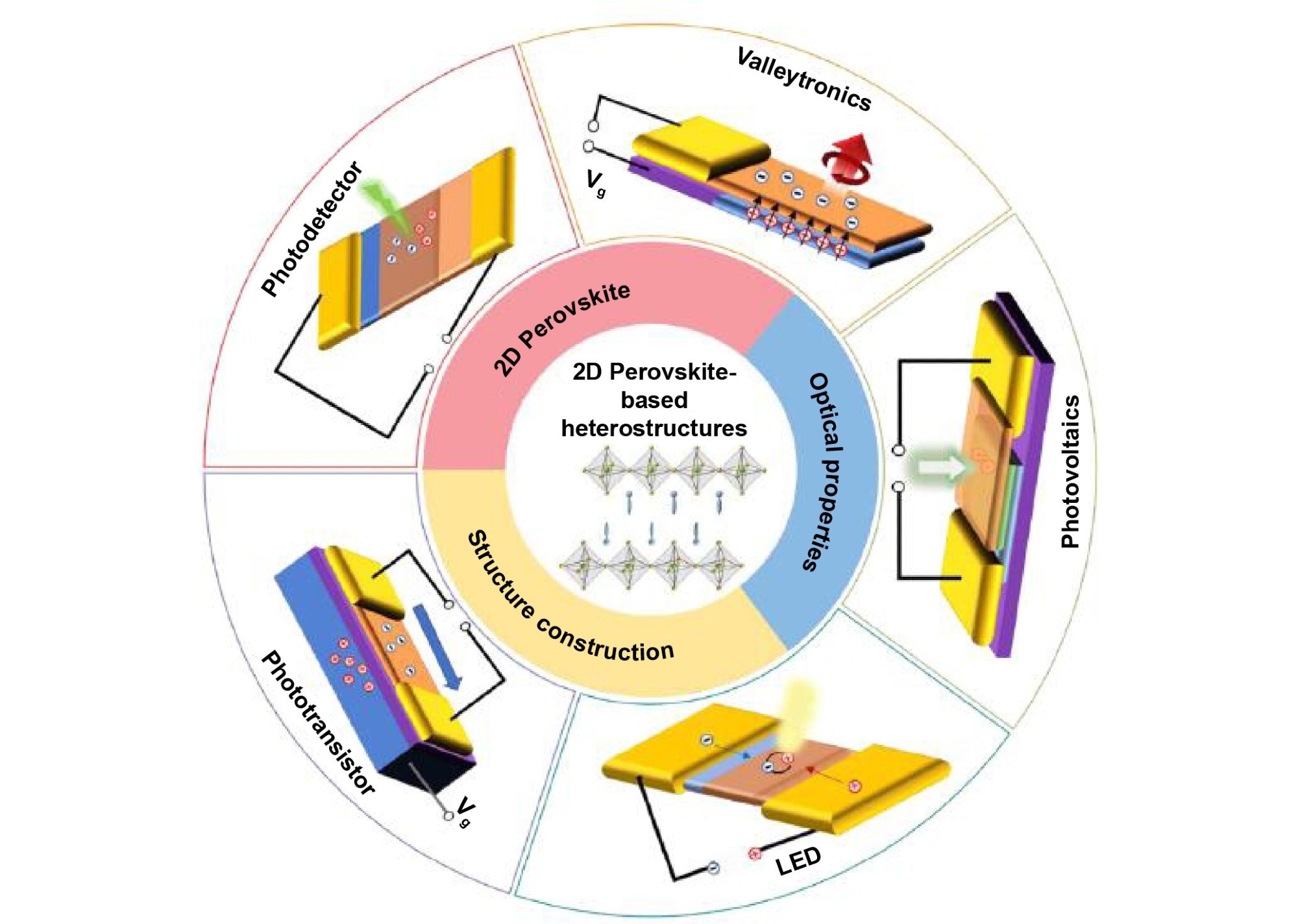
On this article, the construction and bodily properties of 2D perovskites will probably be first highlighted. The development and characterizations of 2D perovskite-based heterostructures in addition to the fundamental optical properties of the constructed heterostructures will then be illustrated. Moreover, the potential functions of 2D perovskite-based heterostructures in photovoltaic units, light-emitting diodes, photodetectors, phototransistors and valleytronic units will probably be demonstrated. Lastly, the present challenges and suggest additional analysis instructions within the discipline of 2D perovskite-based heterostructures will probably be mentioned. Picture Credit score: Haizhen Wang, Yingying Chen and Dehui Li.
A latest research revealed within the Worldwide Journal of Excessive Manufacturing summarizes the latest developments of 2D/quasi-2D perovskite-based heterostructures to expedite the exploration of undiscovered ideas and introduce a brand new spectrum of optoelectronic units.
What are 2D Perovskite-Based mostly Heterostructures?
Heterostructures, that are made by combining two or extra completely different supplies, have been an vital a part of many several types of optoelectronic units, equivalent to photovoltaic cells, light-emitting diodes, and photodetectors.
These buildings are distinctive as a result of they show bodily properties that can not be seen in particular person elements. By combining these supplies, new functionalities might be achieved and explored. Lately, the development of expertise has allowed scientists to make use of atomically skinny supplies equivalent to graphene, black phosphorus, and 2D perovskites to assemble heterostructures.
These supplies have particular bodily and optoelectronic properties that may be additional manipulated with methods equivalent to doping and exterior fields like pressure or electrical fields. 2D perovskites, specifically, have been gaining a variety of consideration resulting from their glorious properties and potential functions in next-generation optoelectronic units.
With the power to include several types of perovskites into heterostructures, there’s a huge vary of latest potentialities for optoelectronic units and functions. Summarizing the analysis progress on these heterostructures may help result in discoveries and developments within the discipline.
Progress on 2D Perovskite-Based mostly Heterostructures: A Literature Hole
Regardless of the rising curiosity in 2D perovskite-based heterostructures resulting from their distinctive optical and optoelectronic properties, there may be nonetheless a scarcity of complete evaluation articles on this discipline.
Presently, revealed evaluation research have targeting heterostructures primarily based on 3D perovskites with 2D morphologies (as an illustration, methylammonium lead triiodide sheets or nanoplatelets) or van der Waals nanocomposites primarily based on 2D Ruddlesden-Popper (RP) perovskite supplies.
Nevertheless, when it considerations heterostructures primarily based on 2D perovskite supplies with layered and non-layered substances equivalent to Alumina (Al2O3), 3D perovskites, and transition metallic dichalcogenides (TMDs), there may be nonetheless a niche within the literature.
Subsequently, it is very important summarize the latest progress made within the discipline of 2D perovskite-based heterostructures, together with essentially the most up to date analysis outcomes and overlaying a broader vary of content material in comparison with beforehand reported evaluation articles.
Highlights of the Present Assessment
On this research, the authors current a complete overview of the most recent developments in 2D perovskite-based heterostructures. The evaluation focuses on the distinctive construction and bodily properties of 2D perovskites and the way they are often utilized to create heterostructures with enhanced optoelectronic properties.
The authors start by emphasizing the layered nature of 2D perovskites, which permits for the creation of skinny flakes that may be mixed with different supplies to kind heterostructures. This mix results in the inheritance of the wonderful optoelectronic properties of 2D perovskites whereas additionally introducing new functionalities.
The authors then describe the development and characterization of 2D perovskite-based heterostructures, highlighting the fundamental optical properties of those supplies.
Additionally they present a radical overview of the potential functions of those supplies in varied optoelectronic units, together with light-emitting diodes, photovoltaic cells, phototransistors, photodetectors, and valleytronic units.
The lead researcher, Professor Dehui Li, commented
The wealthy digital and optical physics provided by 2D perovskites renders them to be very promising for optoelectronic functions.
Future Outlook
Regardless of the numerous progress made within the discipline of 2D perovskites and their heterostructures, way more investigation continues to be wanted to completely perceive their potential. Particularly, a number of areas require additional exploration.
Firstly, acquiring high-quality pure-phase 2D perovskites with many layers is important for developing high-quality heterostructures. Presently, it’s difficult to synthesize very pure section perovskites with numerous layers, which hinders the extraction of intrinsic bodily properties of 2D perovskites.
There’s additionally a must develop an environment friendly artificial methodology for acquiring large-area, high-quality 2D perovskite heterostructures with a controllable development orientation. Presently, no common methodology exists for rationally synthesizing large-scale heterostructures with excessive crystalline high quality.
The wealthy physics of 2D perovskite-based heterostructures is generally unexplored and must be systematically studied for potential optoelectronic functions. For instance, the consequences of natural cations on cost and electron-phonon interplay must be clarified to optimize the efficiency of optoelectronic units.
Lastly, there’s a important alternative to research optoelectronic options primarily based on 2D perovskite heterostructures in addition to different layered supplies. Further options and present traits could also be acquired by stacking various supplies collectively to generate heterostructures and multi-heterostructures.
In conclusion, 2D perovskite heterostructures maintain a lot promise for varied optoelectronic functions, however a lot work nonetheless must be carried out to completely notice their potential.
Reference
Wang, H. et al. (2023). Two/Quasi-two-dimensional perovskite-based heterostructures: development, properties, and functions. Worldwide Journal of Excessive Manufacturing. Out there at: https://doi.org/10.1088/2631-7990/acab40


