| Dec 16, 2022 |
|
(Nanowerk Information) Researchers have developed a brand new all-optical technique for driving a number of extremely dense nanolaser arrays. The method might allow chip-based optical communication hyperlinks that course of and transfer information sooner than immediately’s electronic-based units.
|
|
“The event of optical interconnects geared up with high-density nanolasers would enhance data processing within the information facilities that transfer data throughout the web,” mentioned analysis workforce chief Myung-Ki Kim from Korea College. “This might enable streaming of ultra-high-definition motion pictures, allow larger-scale interactive on-line encounters and video games, speed up the growth of the Web of Issues and supply the quick connectivity wanted for giant information analytics.”
|
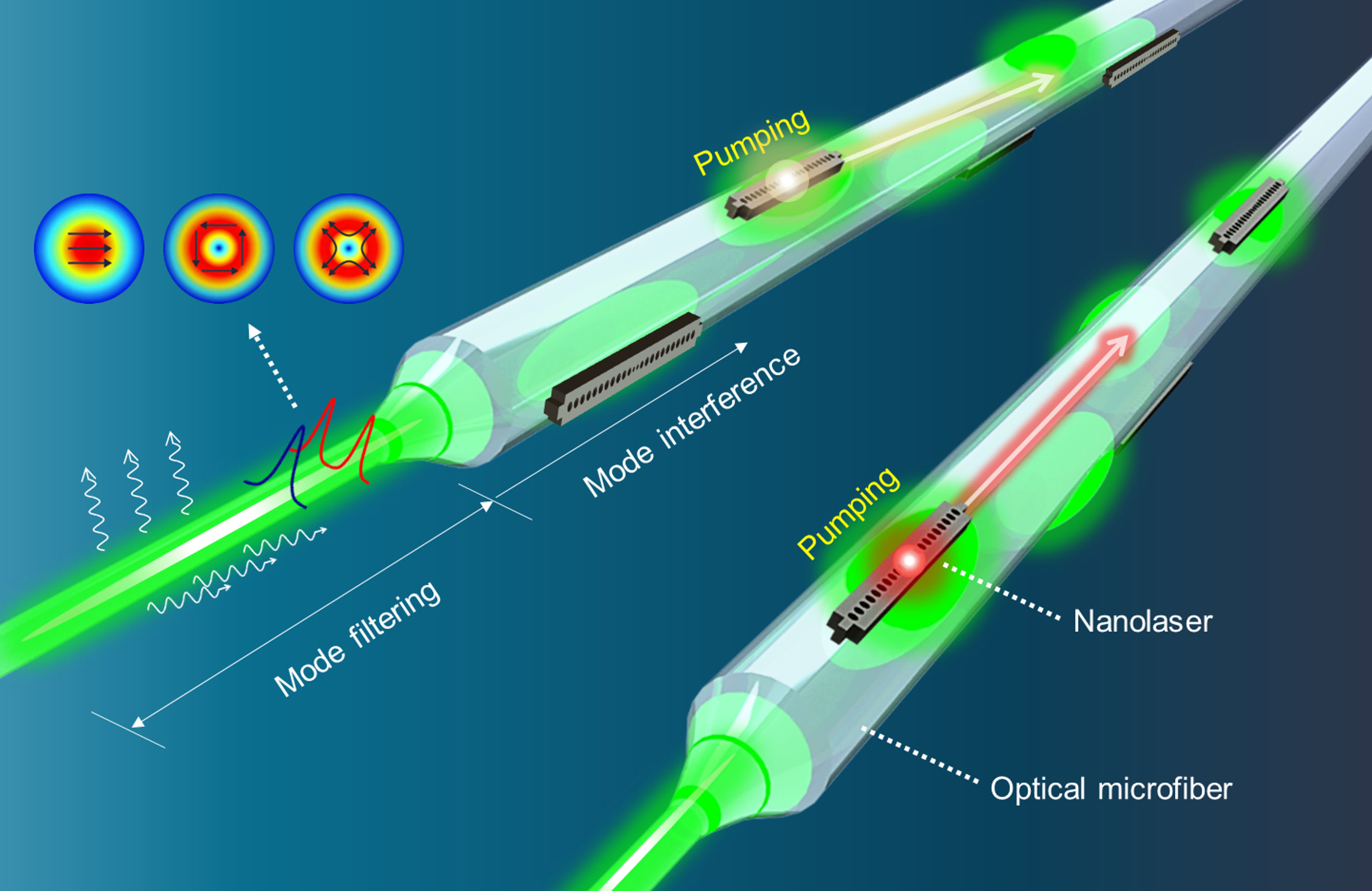 |
| Researchers have developed a brand new all-optical technique for driving a number of excessive density nanolaser arrays utilizing mild touring down a single optical fiber. The optical driver creates programmable patterns of sunshine by way of interference. (Picture: Myung-Ki Kim, Korea College)
|
|
In Optica (“Three-dimensional programming of nanolaser arrays by way of a single optical microfiber”), the researchers show that densely built-in nanolaser arrays — during which the lasers are simply 18 microns aside — might be absolutely pushed and programmed with mild from a single optical fiber.
|
|
“Optical units built-in onto a chip are a promising various to digital built-in units, that are struggling to maintain up with immediately’s information processing calls for,” mentioned Kim. “By eliminating the big and complicated electrodes sometimes used to drive laser arrays, we decreased the general dimensions of the laser array whereas additionally eliminating the warmth technology and processing delays that include electrode-based drivers.”
|
Changing electrodes with mild
|
|
The brand new nanolasers could possibly be utilized in optical built-in circuit techniques, which detect, generate, transmit and course of data on a microchip by way of mild. As an alternative of the effective copper wires utilized in digital chips, optical circuits use optical waveguides, which permit a lot larger bandwidths whereas producing much less warmth. Nevertheless, as a result of the dimensions of optical built-in circuits is shortly reaching into the nanometer regime, there’s a want for brand new methods to drive and management their nano-sized mild sources effectively.
|
|
To emit mild, lasers should be provided with vitality in a course of known as pumping. For nanolaser arrays, that is sometimes achieved utilizing a pair of electrodes for every laser inside an array, which requires important on-chip area and vitality consumption whereas additionally inflicting processing delays. To beat this essential limitation, the researchers changed these electrodes with a novel optical driver that creates programmable patterns of sunshine by way of interference. This pump mild travels by way of an optical fiber onto which nanolasers are printed.
|
|
To show this method, the researchers used a high-resolution transfer-printing method to manufacture a number of photonic crystal nanolasers spaced 18 microns aside. These arrays have been utilized onto the floor of a 2-micron-diameter optical microfiber. This needed to be performed in a approach that exactly aligned the nanolaser arrays with the interference sample. The interference sample is also modified by adjusting the driving beam’s polarization and pulse width.
|
Laser driving with a single fiber
|
|
The experiments confirmed that the design allowed a number of nanolaser arrays to be pushed utilizing mild touring by way of a single fiber. The outcomes matched nicely with numerical calculations and confirmed that the printed nanolaser arrays could possibly be absolutely managed by the pump beam interference patterns.
|
|
“Our all-optical laser driving and programming expertise will also be utilized to chip-based silicon photonics techniques, which might play a key position within the growth of chip-to-chip or on-chip optical interconnects,” mentioned Kim. “Nevertheless, it could be essential to show how independently the modes of a silicon waveguide might be managed. If this may be performed, it could be an enormous leap ahead within the development of on-chip optical interconnects and optical built-in circuits.”
|
",
type: "opt-in",
theme: "edgeless",
palette: {
popup: {
background: "#eee",
text: "#889"
},
button: {
background: "#58f",
text: "#fff"
}
},
content: {
link: "Сookie policy",
allow: "Got it!",
deny: " ",
href: "https://www.nanowerk.com/cookie_policy.php"
},
onInitialise: function(status) {
if(status == cookieconsent.status.allow) myScripts();
},
onStatusChange: function(status) {
if (this.hasConsented()) myScripts();
}
})
});
function myScripts() {
// Paste here your scripts that use cookies requiring consent. See examples below
// Google Analytics, you need to change 'UA-00000000-1' to your ID
(function(i,s,o,g,r,a,m))(window,document,'script','//www.google-analytics.com/analytics.js','ga');
ga('create', 'UA-00000000-1', 'auto');
ga('send', 'pageview');
// Facebook Pixel Code, you need to change '000000000000000' to your PixelID
!function(f,b,e,v,n,t,s)
{if(f.fbq)return;n=f.fbq=function(){n.callMethod?
n.callMethod.apply(n,arguments):n.queue.push(arguments)};
if(!f._fbq)f._fbq=n;n.push=n;n.loaded=!0;n.version='2.0';
n.queue=[];t=b.createElement(e);t.async=!0;
t.src=v;s=b.getElementsByTagName(e)[0];
s.parentNode.insertBefore(t,s)}(window, document,'script',
'https://connect.facebook.net/en_US/fbevents.js');
fbq('init', '000000000000000');
fbq('track', 'PageView');
}


